
Institute for Molecular Science-led team develops atom-holography microscope for 3D atomic imaging
This digest was compiled by AI from multiple sources — links to the originals are below.
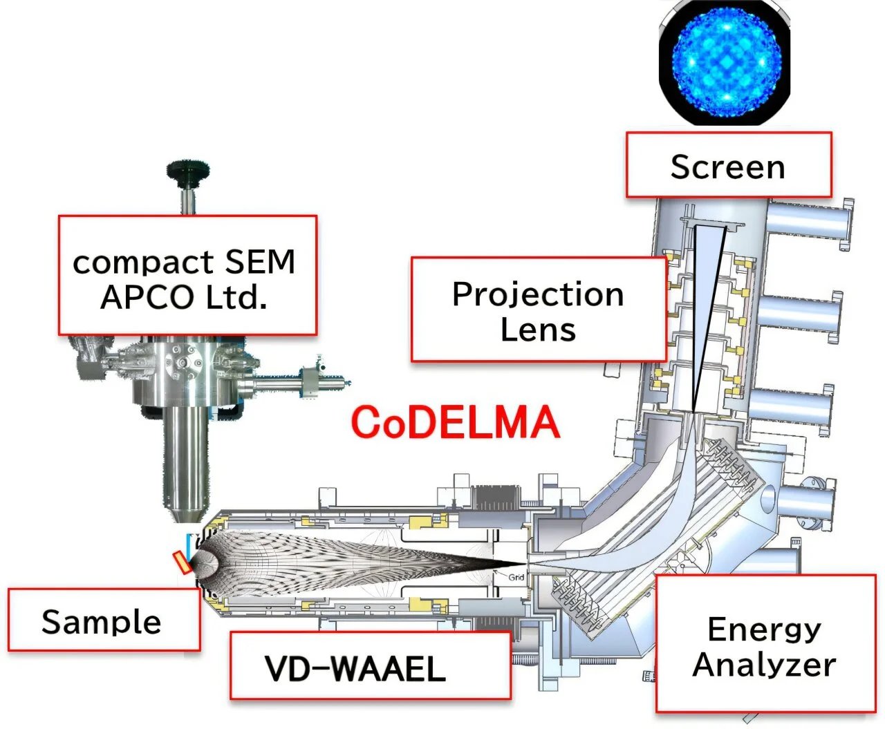
Researchers at the National Institutes of Natural Sciences' Institute for Molecular Science have developed an atom-holography microscope that directly visualizes three-dimensional atomic arrangements in nanoscale regions. The microscope combines an electron beam from a scanning electron microscope with the CoDELMA two-dimensional display-type analyzer to capture holographic angular distributions of emitted electrons. The advance, published in the Review of Scientific Instruments, eliminates the need for synchrotron radiation, making atomic-resolution holography accessible in ordinary laboratories.
Microscope Design
The microscope directs an electron beam from a compact scanning electron microscope onto the sample. The custom-built CoDELMA analyzer focuses electrons emitted over a ±50° angular range into an energy analyzer, which extracts electrons of a selected energy. A projection lens then simultaneously measures their angular distribution, generating a holographic pattern. Computer reconstruction of this hologram reveals the three-dimensional atomic structure around atoms of a specific element.
Synchrotron Independence
Until now, atomic-resolution holography required synchrotron radiation, involving lengthy application processes and restricting measurements to specialized facilities. The new device uses electron-beam excitation, enabling such measurements in any research laboratory. Moreover, the electron beam can be focused to a nanometer-scale spot, allowing atomic-structure analysis within extremely small regions—a capability not possible with synchrotron-based techniques.
Materials Research Boost
Three-dimensional atomic arrangements in nanoscale volumes are critical for developing advanced nanodevices and functional materials. Existing transmission electron microscopy methods produce only two-dimensional projections from thin sections. The element-specific 3D imaging offered by the atom-holography microscope could accelerate progress in semiconductors, catalysts, and quantum materials research.
1 source
Time · lag behind first